
Oxygen Plasma Photoresist Stripping Process in Semiconductor Fabrication
The manufacturing process for integrated circuit (IC) chips or MEMS devices may require 10 to 40 masking steps, each requiring a photoresist stripping process. Dry ashing, or plasma stripping using oxygen plasma, has become the preferred method due to its precision, high throughput, and compatibility with various substrates.
Dry Plasma Ashing Mechanism and Process Fundamentals
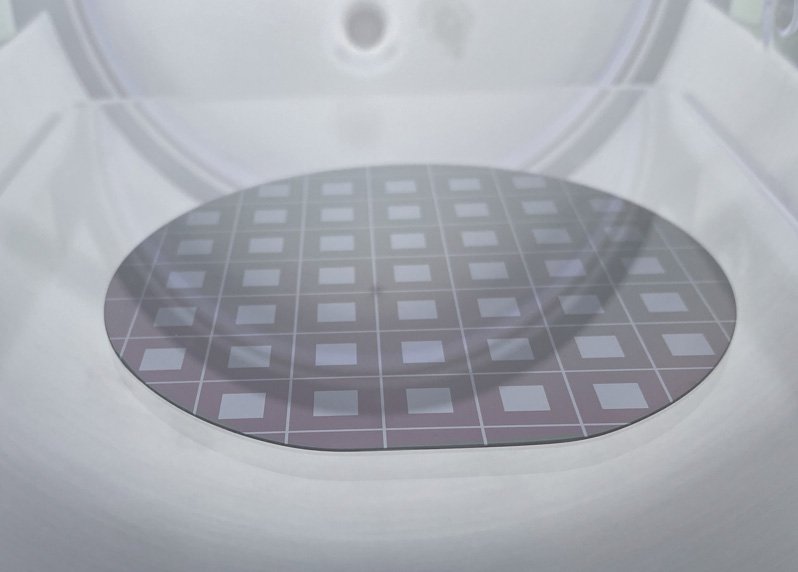
Dry plasma ashing involves exposing the wafer to reactive oxygen plasma in a vacuum environment. The plasma is generated by energizing oxygen gas using radio-frequency (RF) or microwave power, creating a partially ionized gas rich in reactive species. Among these, neutral oxygen radicals (O•) are the primary agents that break down the organic photoresist, converting it into volatile byproducts such as CO, CO₂, and H₂O vapor.
The fundamental reaction is an oxidative breakdown of the polymer chains forming the resist, effectively “burning” the organic material in a low-pressure, high-temperature environment. The vacuum system then evacuates the resulting gaseous byproducts from the chamber.

Typical Process Parameters
Plasma ashing systems typically operate at a 13.56 MHz RF frequency or use microwave sources to generate the intense plasma required for effective photoresist removal—lower-cost kHz RF power simply does not provide sufficient intensity. In addition to RF frequency, plasma system design, discharge mechanism (e.g., CCP, ICP, or microwave), RF power wattage, and operating chamber pressure all influence the plasma’s characteristics. Here are the typical process parameters for the plasma photoresist stripping process:
- Gas Composition: Pure O₂ or O₂ with additives like CF₄ or H₂, depending on photoresist type
- Pressure: Typically 0.25–2.0 Torr
- RF Power: 100–500 W for single-wafer tools
- Temperature: 100–200 °C during ashing
- Plasma Configuration: Downstream or in-situ, depending on substrate sensitivity
Downstream or remote plasma sources can prevent damage from ions and UV radiation. In these setups, plasma is generated away from the wafer, and only neutral radicals (with minimal charged species) reach the wafer surface. This ensures minimal damage to sensitive device layers.
Traditional wet photoresist stripping process
Traditional wet stripping methods rely on organic solvents such as N-methyl-2-pyrrolidone (NMP) or dimethyl sulfoxide (DMSO) to dissolve photoresist films. These solvents, typically applied through heated baths or spray systems, penetrate and swell the resist, facilitating its removal. Additives like hydroxylamine are often used to enhance solubility, particularly for cross-linked or hardened resists.
While effective, wet stripping generates hazardous chemical waste and requires costly disposal procedures. Additionally, the solvents themselves are expensive, contributing to the overall operational costs.
In contrast, the oxygen plasma stripping process uses only industrial-grade oxygen gas to remove photoresist layers. The process produces no hazardous waste, making it significantly more environmentally friendly. It also offers substantial cost savings in both chemical usage and waste management.
Plasma Ashing Equipment Overview
A typical dry plasma ashing system includes the following components:
- Vacuum chamber
- Oxygen gas inlet and mass flow controllers
- RF or microwave power source to generate plasma
- Plasma source (in-situ or downstream)
- Optical endpoint detection system and or Langmuir probe for plasma diagnostics
- Vacuum pump system for byproduct removal
In the single wafer process, the wafer can be loaded with photoresist side directly facing the oxygen radical flow. The single-wafer process usually has a much higher ashing speed. In a multiple wafer process, the wafers can be loaded on a quartz wafer boat and directly placed inside the plasma chamber. The process chamber pressure should be higher than 1 Torr to reduce the mean-free-path so that oxygen radicals can reach the gap between wafers and ensure good uniformity in the multi-wafer process.

Optical Plasma Emission Endpoint Detection
Optical endpoint detection for plasma photoresist stripping leverages Optical Emission Spectroscopy (OES) to monitor the ashing process in real time. As the photoresist oxidizes in the plasma, it generates volatile byproducts such as CO, CO₂, and small hydrocarbon fragments that emit light at characteristic wavelengths (for example, CO around 483 nm/520 nm and hydrogen at 486 nm/657 nm). During the bulk ashing phase, the intensity of these emissions is strong; however, as the resist is nearly depleted, the concentration of carbon-based species drops, leading to a rapid decline or plateau in the optical signal.

An optical fiber collects the plasma light and directs it to a spectrometer, where specialized software continuously analyzes the emission intensity. The system determines the process endpoint when the signal stabilizes or diminishes, ensuring the resist is removed entirely. This method prevents over-ashing, which could damage underlying films, and avoids under-stripping that leaves residues, thereby enhancing process control and overall wafer quality.

Advantages of Dry Plasma Ashing Over Wet Stripping Method
Dry plasma stripping is widely adopted due to several key benefits:
1. High Selectivity and Material Compatibility. Dry ashing targets organic materials like photoresist with minimal interaction with inorganic substrates such as Si, SiO₂, or Si₃N₄. Unlike some wet chemical strippers, it avoids chemical attack on metals or dielectrics.
2. No Risk of Pattern Collapse. Since the process is dry, no surface tension-induced collapse of high-aspect-ratio features can occur during liquid drying in wet processes.
3. Environmental Safety. Plasma processes generate mainly CO₂ and H₂O, with minimal hazardous chemical waste. This eliminates the handling, disposal, and environmental hazards associated with solvents like NMP or DMSO.
4. High Throughput and Integration. Modern single-wafer plasma strip tools can process wafers in under 60 seconds. These tools are often integrated with etch or lithography clusters for streamlined workflow.
5. Process Control with Real-Time Endpoint Detection Optical emission endpoint detection enhances yield and consistency by terminating the process precisely at the point of complete resist removal
Summary
Dry ashing using oxygen plasma is a foundational process in modern semiconductor fabrication, offering high selectivity, cleanliness, environmental safety, and compatibility with delicate device structures. The integration of optical emission endpoint detection further enhances process reliability, ensuring that photoresist is removed precisely and consistently.
As device geometries shrink and materials become more complex, plasma strip tools continue to evolve—with advanced plasma sources, improved uniformity, and hybrid chemistries—enabling fabs to meet ever-tightening performance and yield requirements.
References
- Mack, C. A. (2007). Fundamentals of Lithography. Wiley.
- Chen, J. et al. (2011). “Advances in Plasma Ashing for Semiconductor Processing.” J. Vac. Sci. Technol. B.
- Lee, S. et al. (2013). “Chemical Stripper Formulations and Their Impact on Advanced Patterning.” Microelectron. Eng.
- Li, K. et al. (2018). “Optical Emission Spectroscopy for Endpoint Detection in Plasma Etch and Strip Processes.” IEEE Trans. Semicond. Manuf.
- Park, Y. et al. (2021). “Low-Damage Plasma Strip for Sub-5 nm Logic Devices.” Proc. SPIE 11612, Advanced Etch Technology for Nanopatterning.